Theme: Theme : Probing Innovations and Extending Frontiers in Nano Technology
Materials and Nano Science Congress 2020
About Conference :
We welcome you and appreciate your participation at the 9th Annual Congress on Advanced Materials and Nano Science, which is going to be held during October 26-27, 2020 through Webinar and will be organized around the theme " Probing Innovations and Extending Frontiers in Nano Technology ".
On this great gathering, Organizing Committee invites participants from all over the globe to take part in this annual conference. Materials and Nano Science Congress 2020 aims at sharing new ideas and new technologies amongst the professionals, industrialists and students from research areas of Advanced Materials and Nanotechnology to share their recent innovations and applications and indulge in interactive discussions and technical sessions at the event. The Conference will also have a space for companies and/or institutions to present their services, products, innovations and research results.
Conference Series LLC Ltd., conferences has taken the initiative to gather the world class experts both from academic and industry in a common platform at its Materials and Nano Science Conferences to share their recent research finding to the world and enlighten other esteemed delegates on latest trends in the field of nanotechnology and advanced materials. Materials and Nano Science Congress 2020 is fourth in its series of annual scientific events aimed to provide an opportunity for the delegates to meet, interact and exchange new ideas in the various areas of Nanotechnology.
Materials and Nano Science Congress 2020 is an exciting opportunity to showcase the new technology, the new products of your company, the service your industry may offer to a broad international audience. It covers a lot of topics and it will be a nice platform to showcase their recent researches on Nanotechnology, Material Science and other interesting topics.
Materials and Nano Science Congress 2020 is intended to honor prestigious award for talented Young researchers, Scientists, Young Investigators, Post-Graduate students, Post-doctoral fellows, Trainees, Junior faculty, Professors and technical staff in recognition of their outstanding contribution towards the conference theme. The Young Scientist Awards make every effort in providing a strong professional development opportunity for early career academicians by meeting experts to exchange and share their experiences on all aspects of Nanotechnology.
Importance and Scope :
Materials and Nano Science Congress 2020 plays a vital role in our lives because of its uniqueness in properties and extended application in various industries. These are the basis of modern science and technology. Material and Nano Science are at the heart of many technological developments that touch our lives and find applications such as electronic materials for communication and information technology, biomaterials for better health care, sensors for intelligent environment, energy materials for renewable energy and environment, light alloys for better transportation, materials for strategic applications and more.
Advanced Material and Nano Science is the study of all of the materials we see around us every day. Materials Science or Nano Engineering forms a bridge between the sciences and engineering. It allows theory to be put into practice in a way which benefits everybody. They develop new materials for new applications, improve existing materials to give improved performance and look at ways in which different materials can be used together.
The study further emphasizes the development of relevant skills and IP regulations as well as testing and prototyping facilities. The study aimed to provide the Government, including the data, with strategic recommendations on how this sector can be enhanced in producing new commercial products and process while maximizing the societal benefits.
Why to attend?
Materials and Nano Science Conference offers a fantastic opportunity to meet and make new contacts in the field of Materials Science and Engineering, by providing collaboration spaces and break-out rooms with tea and lunch for delegates between sessions with invaluable networking time for you. It allows delegates to have issues addressed on Materials and Nano Science by recognized global experts who are up to date with the latest developments in the Materials and Nano Science field and provide information on new techniques and technologies. This International Materials and Nano Science conference will feature world renowned keynote speakers, plenary speeches, young research forum, poster presentations, technical workshops and career guidance sessions.
Target Audience :
- Materials Scientists / Research Professors
- Nano Technology Scientists / Research Professors
- Materials Science Engineers
- Nanotechnology Engineers
- Physicists/Chemists
- Research Scholars and students
- Laurets
- Junior/Senior research fellows of Materials Science/ Nanotechnology/ Polymer Science
- Materials and Nano Science Students
- Directors of chemical companies / Nano Tech companies
- Nanotechnology and Material Science Companies
- Nanotechnology and Material Science Associations
- Engineering Professors and Faculty
- Medical Devices software Developer Companies
- Polymer Companies.

There are different requirements to obtain a Visa to enter Europe or other countries. Meeting all visa and customs requirements is an individual responsibility of each participant. Please consult the European Embassy in your country to find out whether you require a visa, and if so, what requirements are set forth for obtaining it. Some embassies may request a conference attendee to present a letter from the Conference to verify their intentions to attend that specific conference. It may also be necessary to verify that the requester has paid the registration fee in full.
Visa applications are currently subject to a greater degree of scrutiny than in the past. Many applicants may be required to appear in person for an interview as a part of the visa process. Applicants affected by these procedures are informed of the need for additional screening at the time they submit their application and are being advised to expect delays. Therefore, attendees should be advised to apply no later than 3 months prior to the conference.
Conferenceseries LLC Ltd guidelines for providing visa letters are as follows:
Visa letters should only be issued to:
• People the committee knows
• Speakers/Presenters
• Committee members
• Attendees who have paid their registration fee in full or as decided by the committee members
Visa letters should state the following facts:
• Conference title, dates and location
• That the requester has paid the required registration fee in full
• Verify that the credit card clears before providing letter
• If they are either a committee member, speaker or presenter
To simplify the request process for the attendees and organizers you need to request for visa letters for the conference once you are done with registration. Official invitation letter along with payment receipt will be mailed to you within 24-48 hours of your confirmation.
For any queries feel free to send us an email at advancematerials@conferencesmeet.com and we shall assist you with more information.
Sessions / Tracks :
Materials and Nano Science Congress 2020 is comprised of various tracks and sessions designed to offer comprehensive sessions that address current issues in the field of Materials Science.
Advanced Materials is an acclaimed scientific discipline, expanding in recent decades to surround polymers, ceramics, glass, composite materials and biomaterials. Materials science and engineering, involves the discovery and design of new materials. Many of the most pressing scientific problems humans currently face are due to the limitations of the materials that are available and, as a result, major breakthroughs in materials science are likely to affect the future of technology significantly. Materials scientists lay stress on understanding how the history of a material influences its structure, and thus its properties and performance. All engineered products from airplanes to musical instruments, alternative energy sources related to ecologically-friendly manufacturing processes, medical devices to artificial tissues, computer chips to data storage devices and many more are made from materials. In fact, all new and altered materials are often at the heart of product innovation in highly diverse applications. The global market is projected to reach $6,000 million by 2020 and lodge a CAGR of 10.2% between 2015 and 2020 in terms of worth. The North American region remains the largest market, accompanied by Asia-Pacific. The Europe market is estimated to be growth at a steady rate due to economic redeem in the region along with the expanding concern for the building insulation and energy savings.
New electronic and photonic Nano materials assure dramatic breakthroughs in communications, computing devices and solid-state lighting. Current research involves bulk crystal growth, organic semiconductors, thin film and nanostructure growth, and soft lithography along with researches related to Optics. Several of the major photonics companies in the world views on different technologies and opinions about future challenges for manufacturers and integrators of lasers and photonics products. The silicon photonics market is anticipated to grow to $497.53 million by 2020, expanding at a CAGR of 27.74% from 2014 to 2020. The silicon carbide semiconductor market is estimated to grow $3182.89 Million by 2020, at an expected CAGR of 42.03% from 2014 to 2020.
Carbon is connected with about all that we see around us. Due to its remarkable properties, like high robustness at normal conditions, differing hybridizations, strong covalent bond game plan and straightforward of blends advancement, carbon has been of consistent excitement for a couple of districts. A nanostructure is a structure of fair size among minute and nuclear structures. Nano structural detail is microstructure at Nano scale.
Graphene is an allotrope of carbon as a two-dimensional, atomic scale, hexagonal cross segment in which one particle shapes each vertex. It is the basic helper segment of various allotropes, including graphite, charcoal, carbon nanotubes and fullerenes. It can moreover be considered as an uncertainly significant sweet-noticing iota, an authoritative occurrence of the gathering of level polycyclic fragrant hydrocarbons.
Material science has a wider range of applications which includes ceramics, composites and polymer materials. Bonding in ceramics and glasses uses both covalent and ionic-covalent types with SiO2 as a basic building block. Ceramics are as soft as clay or as hard as stone and concrete. Usually, they are crystalline in form. Most glasses contain a metal oxide fused with silica. Applications range from structural elements such as steel-reinforced concrete, to the gorilla glass. Polymers are also an important part of materials science. Polymers are the raw materials which are used to make what we commonly call plastics. Specialty plastics are materials with distinctive characteristics, such as ultra-high strength, electrical conductivity, electro-fluorescence, high thermal stability. Plastics are divided not on the basis of their material but on its properties and applications.
Nano Technology is the science deals with the acute very little particles or one dimension sized particles from one to 100nm said as Nano particles. All these particles have the facility to manage individual atoms and molecules. Thanks to the assorted potential applications wide variety of study goes beneath the Nanotechnology throughout the globe like surface science, biology, chemistry, semiconductor physics, energy storage, tiny fabrication, molecular engineering, etc.
Nano Technology is plot in light of the way that the science deals with the extreme little particles or one estimation evaluated particles from one to a hundred nm insinuated as Nano particles. These particles can supervise solitary particles and molecules. inferable from the diverse potential applications wide assurance of examination goes underneath the Nano development all through the world like surface science, substance science, natural science, semiconductor material science, essentialness amassing, little creation, sub-nuclear structure, etc.
Nanoparticles are particles which lie between 1 and 100 nanometers (nm) in size with a surround with layer called interfacial layer. This interfacial layer is an important part of Nano scale matter, essentially affecting all of its properties. This layer typically consists of ions, inorganic and organic molecules. It also use coating inorganic nanoparticles is known as stabilizers, capping and surface ligands, or passivizing agents. They frequently possess unexpected optical properties as they are small enough to limit their electrons and yield quantum effects. Nanoparticles in clay combined into polymer mediums increase reinforcement, which leads to stronger plastics, provable by a higher glass transition temperature and other mechanical property tests. These particles are rigid and impart their properties to the polymer (plastic). These are also used as attachment in textile fibers which help to create smart and functional clothing.
Smart materials are defined as materials with properties engineered to modify in a skillful method under the impact of external stimuli. These exterior impacts can contain temperature, force, moisture, electric charge, magnetic fields and ph. Nanotechnology is rapidly entering the world of smart materials and taking them to the next level. Piezoelectric materials either yield voltage when stressed or change shape under the impact of an electric charge. Thermo responsive materials are also known as shape memory alloys or shape memory polymers. These materials alter their shape under the influence of the ambient temperature. In the field of medical the use of smart materials that respond to injuries by delivering drugs and antibiotics or by hardening to produce a cast on a broken limb. Energy generation and conservation with highly efficient batteries and energy generating materials.
New electronic and photonic Nano materials assure dramatic breakthroughs in communications, computing devices and solid-state lighting. For any electronic device to operate well, electrical current must be efficiently controlled by switching devices, which becomes challenging approach to systems very small dimensions. This problem must be addressed by synthesizing materials that permit reliable turn-on and turn-off current at any size scale. New electronic and photonic Nano materials assure dramatic breakthroughs in communications, computing devices and solid-state lighting. Current research involves bulk crystal growth, organic semiconductors, thin film and nanostructure growth, and soft lithography. Many major photonics companies in the world views on different technologies and opinions about future challenges for manufacturers and integrators of lasers and photonics products.
Any condensed matter systems whose at least one (out of three) dimension is of the order of nanometer can be considered as Nano scale system. Nanotechnology is branch of science which deals with designing, fabricating and monitoring materials and components with dimensions on the Nano scale, i.e. from 1 to 100 nm. Nanophysics teach how nanotechnology can be used in order to develop new optic and electronic components and new materials for use in communications technology, sensor technology or catalysis. Nano physics is branch of physics which applied at nanometer range in order to get proper result. In Nano range properties of materials changed. Basically at Nano range the surface properties of materials start dominating compare to bulk properties. In surface there are dangling bond which have high surface energy compared to bulk.
Nano chemistry unites – naturally – Nano science and chemistry. It works from the atom up, with the aim of engineering Nano sized materials. They use many methods to formulate and collect small pieces of matter which indicate unique magnetic, electronic, optical, chemical and mechanical actions attributable only to their nanometer size. This science use approach from the synthetic chemistry and the materials chemistry to acquire Nano materials with particular sizes, shapes, surface properties, deformities, self-gathering properties, intended to fulfill particular capacities and uses. Nanomaterial’s can be made from for all objectives and purposes any material, for example, metals, semiconductors and polymers, both in their nebulous and crystalline structures. Its tactics can be utilized to make carbon Nano materials, for example, carbon nanotubes (CNT), Graphene and fullerenes which have picked up consideration as of recently because of their mechanical and electrical properties.
Nano weapon is the tag which identifies the military technology currently under develop which seeks to exploit the power of nanotechnology in the modern battlefield. These particles used in different military materials could possibly hazard in nature to the soldiers that are wearing the material, if the material is allowed to get worn out. As the uniforms wear out it is likely for nanomaterial to separate and enter into the soldiers’ bodies’. Soldiers having nanoparticles arriving the soldiers’ bodies would be very unhealthy and could create seriously harm to them. There is not a lot of information on what the actual damage to the soldiers would be, but there have been studies on the effect of nanoparticles entering a fish through its skin. The studies showed that the different soldiers suffered from varying degrees of brain damage. These brain damage would create serious negative effect; the studies also say that the results cannot be taken as an accurate example of what would happen to soldiers if nanoparticles entered their bodies. There are very strict regulations on the scientists that manufacture products with nanoparticles.
Nano biotechnology refers function which joins nanotechnology and biology. The subject of Nano Biotechnology is one that has only arose very recently and helps as blanket terms for various related technologies. The use of the intrinsic properties of nucleic acids like DNA to create useful materials is a promising area of modern research. This frequently used to define the assemble multidisciplinary actions associated with biosensors, particularly where photonics, chemistry, biology, biophysics, Nano medicine, and engineering converge. Bio nanotechnology is the term that refers to the juncture of nanotechnology and biology. These Ideas which improved through Nano biology are includes with Materials like Nano scale, Nano devices, and nanoparticles phenomena that occurs within the discipline of nanotechnology. Its applications are under research currently, verified and in some cases already applied in different field like food technology, from agriculture to food processing, packaging and food supple.
A nanotube is nanometer-scale tube-like structures, which are also known as nanowires, in terms of feature ratio; but unlike wires, tubes are hollow. Nanotubes maybe single-walled or multi-walled. These wires are in 1D nanostructure which generally has diameters of the tens in order of nanometers, with unrestricted length scales. The length to diameter ratio may be as much as 1000. Nanowires and nanotubes are now at the forefront of materials science at the Nano scale. This article starts with introductory comments about nanowires and nanotubes and then addresses in more detail the special structure and properties of bismuth nanowires and carbon nanotubes, which are considered as prototype examples of nanowires and nanotubes. Both Nano-materials are important for the new Nano science concepts that they introduce and for their promise for practical applications. Both provide a system that is simple enough so that detailed calculations of their properties can be carried out, and predictions about their physical behavior can be made. The occurrence and control of unusual and unique properties of specific nanostructures are the drivers for the exploitation of Nano science in nanotechnology applications.
Nano electronics refer to the usage of nanotechnology on electronic components, particularly transistors. Nano electronics often mention to transistor devices that are so small that inter-atomic relations and quantum mechanical properties need to be studied widely. Theses Nano electronic expedients are manufactured with hybrid molecular/semiconductor electronics, one dimensional nanotubes/nanowires, or advanced molecular electronics. Nano Electronics involves the study of the synthesis and characterization of materials of Nano scale size. It is the combination of chemistry and Nano science. At particularly small level of Quantum effect is very important, fascinating and possibly scientifically very rewarding innovative ways of carrying out chemical reactions are possible. Nanoparticles have the high surface to volume ratio which has intense effect on their properties. This small size of nanoparticles gives them unusual structure and optical properties with applications in catalysis, electro-optical devices, medicine, cosmetics etc.
- Nano Devices and Nano Sensors
Nanodevices, the quickest moving section of the overall market, the Nanotek research includes in smart sensors and smart delivery systems, Magnetic Nano devices, Nano-biosensors, Nano switches, Optical biosensors, and biologically inspired devices are expected to transport at excellent 34% CAGR. Nano sensors will work better on the onset of sicknesses along with cancer or coronary heart ailment, and Nano markets assumes the marketplace for biomedical Nano sensors to reach approximately $800 million in 2019. Around 18 universities and 53 new research initiatives are exhibited in Nanotechnology convention The electrical properties of carbon nanotubes1 (CNTs) and graphene2 make them exceptional candidates for developing novel devices with functionality and efficiency that is orders-of-magnitude better than state-of-the-art technologies. These next-generation electronics will significantly increase the capabilities of high-throughput information systems while simultaneously decreasing their size, weight, cost, and assembly complexity. It also uses to detect various chemicals in gases for pollution monitoring in Atmosphere.
Nano robotics is the technology of making machines or robots at or close to the scale of a nanometer (10-9 meters).Nano robots (Nano bots or Nano Tech) are typically devices ranging in size from 0.1-10 micrometers. As no artificial non-biological Nano robots have so far been created, they remain a theoretical concept at this time. Following this definition even a large apparatus such as an atomic force microscope can be considered a Nano robotic instrument when configured to perform Nano manipulation. Also, micro robots which can move with Nano scale precision can also be considered Nano robots. These machines are largely used in the research and development segment but some primitive molecular machines and Nano motors have been tested. These can then be linked by chemical or physical means to form subassemblies, which in turn can be further manipulated. Applications in building wires, single-electron transistors, and Nano waveguides are presented.
Nanotechnology offers some exciting potentials in medicine Science. Submission of Nanotechnology in Nano medicine involves two main techniques i.e. Diagnostic technique and Therapeutic technique. Nano flares are nanoparticles which are designed bind to genetic targets in cancer cells and generate light when that particular genetic target is found. Nanotechnology provides methods to inactivate specific proteins or genes in cells without genetic changes, to isolate their function. It is a combination of therapeutic and imaging material based on the use of nanoparticles for drug delivery. It will combine imaging with cell-specific therapeutic delivery to allow better evaluation of how medication is reaching its intended target. The other is the impact of nanoparticles in diagnostic assays, which allow precise measurements of concentrations that are orders of magnitude lower than current techniques. Both approaches give an insight into the potential breakthroughs in clinical research that might be accomplished with nanotechnology. Furthermore, the nanotechnology-based methods are emerging as a significant step forward for the easy and rapid analysis of the genetic basis and treatment of diseases. The study comprises a limited number of strategies and a glimpse where the nanotechnology field could evolve.
A biomaterial is any substance that has been engineered to interact with biological structures for a scientific reason - both a therapeutic (treat, augment, repair or substitute a tissue characteristic of the body) or a diagnostic one. As a science, biomaterials is about fifty years old. The learn about of biomaterials is called biomaterials science or biomaterials engineering. It has skilled steady and strong boom over its history, with many businesses investing large quantities of cash into the development of new products. Biomaterials science encompasses elements of medicine, biology, chemistry, tissue engineering and substances science.
Note that a biomaterial is distinctive from a biological material, such as bone, that is produced by a biological system. Additionally, care in exercised in defining a biomaterial as biocompatible, given that it is application-specific. A biomaterial that is biocompatible or appropriate for one application may additionally not be biocompatible in another.
Pharmaceutical Nanotechnology publishes original manuscripts, full-length/mini reviews, thematic issues, speedy technical notes and commentaries that grant insights into the synthesis, characterization and pharmaceutical (or diagnostic) application of substances at the Nano scale. The Nano scale is defined as a measurement range of below 1 µm. Scientific findings related to micro and macro systems with performance residing within facets described at the Nano scale are additionally inside the scope of the journal. Manuscripts detailing the synthesis, exhaustive characterization, biological evaluation, medical testing and/ or toxicological evaluation of Nano materials are of particular pastime to the journal’s readership. Articles ought to be self-contained, centered on a properly based speculation and ought to purpose to exhibit the pharmaceutical/ diagnostic implications of the nanotechnology approach. Manuscripts need to aim, anyplace possible, to demonstrate the in vivo have an effect on of any Nano technological intervention. As reducing a fabric to the Nano scale is capable of essentially altering the material’s properties, the journal’s readership is especially involved in new characterization strategies and the advanced properties that originate from this measurement reduction.
Computational Materials Science goals to augment the communication between tentative materials investigation and computational effort on each surviving and fresh innovative substances and their applications. It circulates articles of interest to physicists, chemists and materials researchers and engineers and to other scientists convoluted by way of skill of computational modeling and substances phenomena. Computational methods already play important part in various substances analyses and will individually come to be extra persistent as laptop manage progresses in the many years ahead. The improvement and utility of techniques are engaged to compute the atomic and digital shape of materials. Computational Materials Science also leveraging novel enlargements in statistics and computer expertise to apprehend composite simulations and accelerate the scheme of materials. Finite Element Method (FEM) is the highest beneficial computational approach for materials associated layout at structural level. Current presentations encompass substances for digital applications, Nano-Electro mechanics and energy. Computational materials science includes computational equipment’s for resolving substances related problems.
Ceramic engineering is the science and science of developing objects from inorganic, non-metallic materials. This is achieved both with the aid of the motion of heat, or at lower temperatures the usage of precipitation reactions from high-purity chemical solutions. The word Ceramics covers inorganic, non-metallic, strong substances that have been hardened via baking at excessive temperature. The most vital of these had been the regular clays, made into pottery, dinnerware, bricks, and tiles. Ceramics have high hardness, high compressive strength, and chemical inertness.
Nano surgery is the time period that refers to surgical treatment that uses fast laser beams which are targeted via goal microscope lens to exert a managed force to manipulate organelles and other subcellular structures .This particular technique permits for the destruction of a single cell except unfavorable adjoining healthful cells. It permits precise ablation of cell and subcellular constructions without compromising telephone viability and with minimal damage to nearby cells.
Conventional Nano surgery makes use of optical tweezers that consists of beams of laser light .The narrowest point of the laser beam includes a strong electric powered subject gradient at the middle that attracts dielectric particles such that they go along the gradient towards the enabling the particles to be moved from one vicinity to another, besides ever touching them. The optical tweezers can be applied to organic substructures such as telephone nuclei and chromosomes. In combination with a scalpel, the optical tweezers permit for even higher precision for the duration of surgery.
Nanofabrication refers to the design procedure of nanomaterial and devices that are measured in nanometers. One nanometer is one millionth (10-9) of a meter. It helps in parallel processing of material over a large scale. It is a cost-effective method whereby large-scale economy is manufactured using the same machinery and design and small amount of material. To meet the continuing challenge of shrinking component size in microelectronics, new tools and techniques are continuously being developed. Component sizes that were in tens of micrometers became single-digit micrometers, and then hundreds of nanometers, and then went down to a few tens of nanometers where they stand today. As a result, what used to be called micro fabrication was rebranded as nanofabrication, although the governing principles have remained essentially the same. The main driver of this technology has been the manufacture of integrated circuits, but there have been tremendous fallout benefits to other areas, including photonics. Nanofabrication can be loosely divided into three major areas: thin films, lithography, and etching. Each of these is vast subject areas in and of themselves, but in this chapter we attempt to cover their essential concepts in a concise fashion for someone new to these areas. The goal is not to provide a working experience that allows one to walk into a laboratory and perform these tasks, but to provide an overall understanding of what these areas are as well as the pros and cons of the most commonly used techniques. Hopefully it will build a foundation for more specific training for anyone who wants to venture further into these areas.
Two dimensional materials, regularly named as single layered crystalline materials comprise of single layer of particles. A considerable research is going on about 2D materials because of their remarkable properties. The progressed 2D materials of intrigue are Grapheme, graphite, Borophene, apropos, silicone, phosphorene, bismuthine and so on. Among the carbon allotropes, grapheme is one of the most adaptable individuals and has been broadly contemplated. Grapheme is in a state i.e., in the middle of and called as a semi metal. In grapheme, electrons/openings act as massless Dirac Fermion as a result of the direct vitality scattering, in this manner portability is seen as high. Grapheme has high optical straightforwardness from close to IR to close to UV subsequently it can supplant indium tin oxide in straightforward leading anodes.
A sharp structure is a system containing multifunctional parts that can perform recognizing, control, and enactment; it is a rough straightforward of a natural body. Clever materials are used to build up these splendid structures, which can perform both identifying and actuation limits. Shrewd materials are new age materials outflanking the standard helper and useful materials. These materials have adaptable abilities to external shocks, for instance, weights or condition, with innate information.
In right now, which is seeing a taking off of essentialness costs and an exponential decrease in the arrangements of non-sustainable power sources, there rises a need to make systems for shrewd use of imperativeness which lay highlight on verifying the earth as well. One of the novel ways to deal with accomplish this is through essentialness gathering. Essentialness social occasion, or imperativeness scavenging, is a technique that gets little proportions of imperativeness that would by one way or another or another be lost as warmth, light, strong, vibration or improvement. It uses this got imperativeness to improve adequacy and to engage new advancement, like remote sensor frameworks. Essentialness gathering also can exchange batteries for little, low control electronic contraptions. Piezoelectric materials can be used as strategies for changing including vibrations into electrical essentialness that would then have the option to be taken care of and used to control various devices.
The Interesting things about nanotechnology are that properties of materials change when the size scale of their dimension reaches nanometers. Manufacturing of materials at Nano scale is done by material scientists to understand the property changes. The field of material science includes characterization and properties of Nano scale materials. Carbon nanotubes are concerned to the elegance of many scientists worldwide. The small proportions, strength and the outstanding physical properties of these arrangements make them very unique material with a whole range of auspicious applications. The prominence in application of computational methods in discovering various sizes of fullerenes and their isomers is given. The theory of isolated pentagon rule in fullerene chemistry has been publicized. Nano photonics collects a large group of faculty members to raise new ideas and to carry out collective research with enhanced stimulation.
Chemical Vapor Deposition has the ability to produce various types of catalytically attractive Nano-scale structures by altering the surface assets of massive or even Nano-divided substrates. Comparatively new processes such as catalytic, fluidized-bed, rotary, two-step and large spot laser CVD allow the creation of nanoparticles, nanotubes, Nano fibers and oriented films. Intensive research is being performed on the production and the preparation of supported catalysts by CVD. Graphene Nano fibers are materials that show amazing properties appropriate for a number of progressive energy storage devices as well as chemical procedures. These solids deal with the direct route for the production of large quantities of high quality Graphene. The cost of manufacturing these supplies on a marketable scale presents a major challenge, which we have pursued to overcome via the usage of natural gas as a source of carbon. Catalysts are divided in to two types homogeneous and heterogeneous. The substance that is constant in composition is termed as homogenous mixture, whereas heterogeneous catalysts are solids that are supplemented in to gas or liquid reaction mixtures.
Material science plays important role in metallurgy too. Powder metallurgy is a term covering a wide range of ways in which materials or components are made from metal powders. They can avoid, or greatly reduce, the need to use metal removal processes and can reduce the costs. Pyro metallurgy includes thermal treatment of minerals and metallurgical ores and concentrates to bring about physical and chemical transformations in the materials to enable recovery of valuable metals. A complete knowledge of metallurgy can help us to extract the metal in a more feasible way and can used to a wider range. Global Metallurgy market will develop at a modest 5.4% CAGR from 2014 to 2020. This will result in an increase in the market’s valuation from US$6 in 2013 to US$8.7 by 2020. The global market for powder metallurgy parts and powder shipments was 4.3 billion pounds (valued at $20.7 billion) in 2011 and grew to nearly 4.5 billion pounds ($20.5 billion) in 2012. This market is expected to reach 5.4 billion pounds (a value of nearly $26.5 billion) by 2017.
Market Analysis :
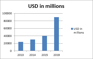
Advanced Materials and Nano Science refers to a wide range of technologies conducted on functional systems at the nanometer scale. It can be said that Advanced materials and Nano science is the ability that can be projected to construct items either using the bottom-up approach or using the top-down approach, whereby top-down Nano Science is considered to be the most well-established form of Nano Science. The global advanced materials and Nano Science market should reach $90.5 billion by 2021 from $39.2 billion in 2016 at a compound annual growth rate (CAGR) of 18.2%, from 2016 to 2021. Thus, there lies a great opportunity for industry participants to tap the fast-growing market, which would garner huge revenue on the back of commercialization of the technology.
9th Annual Congress on Advanced materials and Nano Science 2020 welcomes attendees, presenters & exhibitors from all over the world. The organizing committee is gearing up for an exciting and informative conference program this year also which includes plenary lectures, symposia, workshops on a variety of topics, poster presentations and various programs for participants from all over the world. We are delighted to invite you all to join & register for the international conference on “9th Annual Congress on Advanced materials and Nano Science " which is going to be organized during October 26-27 in through Webinar.
A Glance at Market Value :
The Czech Republic became a part of the NATO in 1999 and the European Union in 2004. It has an open, stable and prosperous market economy with growth led by exports to the EU, especially Germany. The economy has been predominantly privatized following their exit from communism in 1989. The GDP of the nation was reported as $286.7 billion in 2012. The Czech Republic is also recognized as having a rich scientific tradition with numerous inventions originating in the Czech lands.
The given Global Market Size in Czech Republic and is expected to grow in coming years.
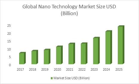
The Global Advanced materials and Nano Science Market is poised to grow at a CAGR of around 18.1% over the next decade to reach approximately $173.95 billion by 2025. This industry report analyzes the global markets for Advanced materials and Nano Science across all the given segments on global as well as regional levels presented in the research scope. The study focuses on market trends, leading players, supply chain trends, technological innovations, key developments, and future strategies. With comprehensive market assessment across the major geographies such as North America, Europe, Asia Pacific, Middle East, Latin America and Rest of the world the report is a valuable asset for the existing players, new entrants and the future investors.
The annual growth in the market size of Advanced materials and Nano Science in recent years.
The 16th International Conference on Emerging Materials and Nanotechnology hosted by conference series, that was successfully command throughout March 22-23, 2018 at London, UK has received an awful and huge participation from scientists, researchers, young researchers from academics and business.
The event has marked a milestone with the colossal and exuberant presence of adepts, young and smart researchers, business delegates and precocious student communities representing quite twenty two countries, golf stroke Emerging Materials and Nanotechnology 2018 among the front row of success with the support from Media Partners-Leedey Physical Institute, Infrasign, PCO and C-locate.
The congregation witnessed many thought agitating and vibrant talks delivered by the eminent and exquisite speakers from the sphere. Each sessions competitive at intervals in excellence, beholded vivacious and vivid discussions promulgating the importance and leading edge analysis on Advanced Materials and Nano Science.
The meeting was allotted through varied scientific sessions, within which the discussions were prevailed the subsequent major scientific sessions.
• Material Science and Engineering
• Materials and Devices
• Emerging Materials for Energy Storage
• Nanotechnology in Materials Science
• Energy Materials
• Surface Science and Engineering
• Materials Characterization
• Polymer Technology
• Electrical, Optical, Magnetic Materials
• Advanced Materials
The event enlightened varied areas of Materials and Nano Science, with Keynote lectures from the skilled speakers of assorted universities and organizations like
Alan J. Russell, Carnegie Mellon University, USA
Pavel Lazarev, Capacitor Sciences Inc., USA
Alberto Tagliaferro, Politecnico Torino, Italy
Dimitris Drikakis, University of Strathclyde, UK
Ludek Frank, Czech Academy of Sciences, CzechRepublic
We are obligated to varied delegate consultants, company representatives and alternative eminent personalities UN agency supported the conference by facilitating active discussion forums. We tend to sincerely convey the Organizing Committee Members for his or her gracious presence, support, and help towards the success of rising Materials and technology 2018.
With the grand success of rising Materials and technology 2018, Conference Series proud to announce the "9th Annual Congress on Advanced Materials and Nano Science” to be held during October 26-27, 2020 through Webinar.
Conference Highlights
- Advanced Materials
- Advanced Optical Materials
- Carbon Based Materials
- Polymer Science and Nano Engineering
- Nano Technology
- Nano Particles
- Nano Materials
- Electronic, Optical and Magnetic Materials
- Nano Physics
- Nano Chemistry
- Nano Weapons
- Nano Biotechnology
- Nano Tubes and Nano Wires
- Nano Electronics
- Nano Devices and Nano Sensors
- Nano Robotics
- Nano Technology in Clinical and Translational Research
- Bio Materials
- Pharmaceutical Nanotechnology
- Computational Material Science
- Ceramic Materials
- Nano Surgery
- Nano Fabrication
- Advanced 2D Materials
- Smart Materials
- Energy Harvesting Materials
- Nano Technology in Material Science
- Catalytic Materials
- Metals and Metallurgy
- Nano Structures
To share your views and research, please click here to register for the Conference.
To Collaborate Scientific Professionals around the World
| Conference Date | October 26-27, 2020 | ||
| Sponsors & Exhibitors |
|
||
| Speaker Opportunity Closed | |||
| Poster Opportunity Closed | Click Here to View | ||
Useful Links
Special Issues
All accepted abstracts will be published in respective Our International Journals.
- Journal of Material Sciences and Engineering
- Journal of Nanosciences
- Journal of Nanomaterials & Molecular Nanotechnology
Abstracts will be provided with Digital Object Identifier by